• Home
  • About Us
  • Breaking News
  • Semiconductor Insights
  • Contact Us
  • Talent Solutions
  • Packaging Solutions
  • Integrated Digital Services
Advanced Packaging Becomes the New Moore’s Law: Why AI Chips Are Scaling Beyond Transistors

Advanced Packaging Becomes the New Moore’s Law: Why AI Chips Are Scaling Beyond Transistors

by admin | Jan 21, 2026 | Executive Search, Semiconductor Packaging Solutions

The race to build smarter, faster AI chips isn’t just about shrinking transistors anymore — the real breakthrough comes from advanced packaging. By combining chiplets, high-bandwidth memory, and Gate-All-Around transistors, the semiconductor industry is rewriting the...
TSMC’s Record-Smashing AI-Fueled Growth: Nvidia-Driven Revenue Beats Estimates, Signals Tech Supercycle Ahead

TSMC’s Record-Smashing AI-Fueled Growth: Nvidia-Driven Revenue Beats Estimates, Signals Tech Supercycle Ahead

by admin | Jan 12, 2026 | Executive Search, Semiconductor Packaging Solutions

TSMC reported a quarterly revenue beat driven primarily by NVIDIA-led AI workloads and advanced-node manufacturing. Q4 revenue rose approximately 20.5% year-on-year to NT$1.046 trillion (US$33.1 billion), fueled by GPUs, AI accelerators, and custom silicon programs....
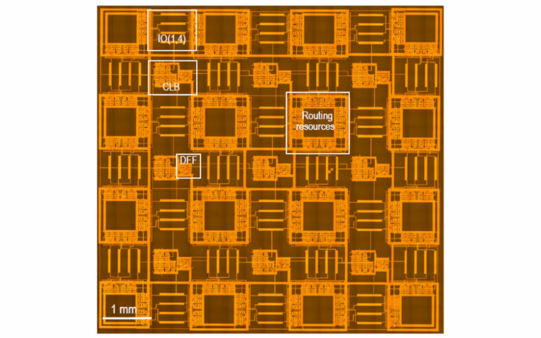
China Achieves Historic Leap with World’s First Radiation-Resistant FPGA Chip Built on 2D Semiconductors

China Achieves Historic Leap with World’s First Radiation-Resistant FPGA Chip Built on 2D Semiconductors

by admin | Nov 6, 2025 | Semiconductor Packaging Solutions

Chinese researchers at Fudan University have developed a 1-nanometre Field-Programmable Gate Array (FPGA) using molybdenum disulfide (MoS₂) that can withstand radiation levels fatal to conventional silicon chips. This breakthrough marks a major advance in 2D...

As Industry Scales to 12-Inch and Square-Panel Wafers, a 2-Inch Superconducting Germanium Breakthrough Signals Another Material Disruption

by admin | Nov 5, 2025 | Semiconductor Packaging Solutions

While the semiconductor world races toward 12-inch wafers and square-panel formats for high-volume production, researchers at New York University and The University of Queensland discovered superconductivity in a 2-inch gallium-doped germanium wafer using standard...
Amazon, OpenAI Forge Game-Changing $38 Billion AI Compute Alliance Powered by NVIDIA GPUs

Amazon, OpenAI Forge Game-Changing $38 Billion AI Compute Alliance Powered by NVIDIA GPUs

by admin | Nov 4, 2025 | Semiconductor Packaging Solutions

Amazon Web Services (AWS) and OpenAI have entered a landmark $38 billion multi-year alliance to expand global AI compute capacity using NVIDIA’s most advanced GPUs. The partnership signals a new phase in the AI infrastructure race where compute power, cloud...
Warren Buffett’s Berkshire Hathaway Amasses Record $381.7 B Cash War Chest, Gains Big from Tech & AI Sector Investments

Warren Buffett’s Berkshire Hathaway Amasses Record $381.7 B Cash War Chest, Gains Big from Tech & AI Sector Investments

by admin | Nov 3, 2025 | Semiconductor Packaging Solutions

Warren Buffett’s Berkshire Hathaway has raised its cash reserves to a historic $381.7 billion, signaling unparalleled liquidity and strategic foresight. This milestone highlights Buffett’s disciplined investing style and shows how selective exposure to technology and...

« Older Entries
Next Entries »

Recent Posts

  • Filtronic Wins $68.1 Million SpaceX Deal: GaN Technology to Power Satellite Communications
  • Wafer Baking in Photoresist Photolithography
  • TSMC To Build 6 More Fabs in Texas?
  • TSMC Reaches the Atomic Frontier: The 0.42-Nanometer Interface That Could Redefine Transistor Scaling
  • SPIL’s $3.1 Billion Bet: Taiwan Builds Next Engine of AI Semiconductor Boom with CoWoS, Set to Create 2,000+ Jobs

Recent Comments

No comments to show.
  • Follow
  • Follow
  • Follow
  • Follow
  • Follow
  • Follow
  • Follow

Office Address

Canberra Crescent, Singapore 752119

Contact Us

  • richard.olivas@tmbsconsulting.com

© Copyright 2024 TMBS Consulting. All Rights Reserved.