
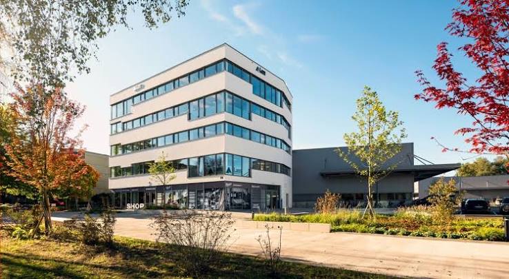
- Lam Researchis entering panel-level packaging with a new Panel-Level Packaging Center of Excellence in Salzburg, Austria, a city in western Austria, as AI and high-performance computing drive demand for larger and more complex semiconductor packages.
- Panel-level packaging uses large square or rectangular substrates instead of traditional circular wafers, creating a larger manufacturing platform that could improve scalability and efficiency for next-generation semiconductor packages.
- Lam Research is a global supplier of semiconductor wafer fabrication equipment and services, with its technologies used across the production of advanced chips worldwide. Its expertise spans systems engineering, process technology and manufacturing equipment, giving Lam Research a significant position as semiconductor packaging evolves from wafer-based processes toward larger panel formats.
- AI is changing the physical economics of advanced packaging as larger dies, denser interconnects, HBM and heterogeneous architectures push package dimensions and complexity higher. Panel-level processing offers a potential path to handling larger package formats while improving substrate utilization and manufacturing scalability.
- Lam Research’s move extends its wet-processing capabilities from wafer manufacturing into panel-level plating, cleaning and etching, bringing chemical process control deeper into the emerging packaging equation. Lam Research’s Kallisto and Phoenix platforms are designed around manufacturability, automation and throughput as panel processing moves closer to production environments.
- The transition from wafer to panel introduces engineering challenges involving uniformity, edge control, warpage, precision, defect management and yield across much larger surfaces. These variables can directly influence manufacturing cost, throughput and the commercial viability of panel-level packaging.
- Lam Research’s Salzburg facility is designed to accelerate R&D, early qualification and customer co-development, shortening learning cycles between experimental processes and manufacturing-ready solutions. Faster iteration can reduce technical risk as semiconductor companies evaluate panel-level processing for future production environments.
- The economic opportunity extends beyond semiconductor equipment because panel-level manufacturing can create demand for substrates, chemicals, carriers, tooling, handling systems, inspection, automation and protective packaging. A shift in package format therefore has the potential to reshape portions of the wider semiconductor supply chain.
- Manufacturing readiness could become a defining factor as panel-level packaging progresses from R&D and pilot stages toward higher-volume production. Process capability, automation, throughput, yield and repeatability will determine how effectively the technology translates from laboratory potential into commercial semiconductor output.
- Panel-level packaging could reshape the economics of the semiconductor business as AI drives demand for larger and more complex packages. The transition could influence capital investment, manufacturing capacity, supplier relationships, production costs and access to new AI-driven revenue opportunities, creating space for companies with the right technology, partners, capabilities and talent to capture emerging value.
- The wafer-to-panel transition is creating a new technical frontier for semiconductor professionals as companies build capabilities ahead of widespread manufacturing adoption. Engineers and leaders able to combine advanced packaging knowledge with process control, equipment, automation, yield and manufacturing economics could find new pathways for technical specialization, leadership and career growth as the packaging ecosystem expands.
TMBS Consulting – Your Semiconductor Concierge
At TMBS Consulting, we connect organizations with the best-fit Senior Management leaders, Professionals, and Technical Staff to strengthen engineering capability, manufacturing excellence, and business growth—from advanced packaging and semiconductor manufacturing to emerging technologies such as panel-level packaging.
We also deliver high-quality carrier tapes, cover tapes, reels, and thermoforming trays tailored for the industry’s most in-demand and advanced semiconductor packages—from PDIP, SOIC, QFN, and WLCSP to chiplets, modules, and panel-level packaging.
📩 DM us today.
#LamResearch #PanelLevelPackaging #AdvancedPackaging #SemiconductorPackaging #AI #HighPerformanceComputing #Chiplets #SemiconductorIndustry #SemiconductorJobs #TMBSConsulting