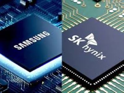
- eports that Samsung Group and SK Group are expected to unveil investment plans worth up to US$1.3 trillion over the next decade briefly sent shares of Samsung Electronics and SK hynix lower, reminding investors that markets often react cautiously to massive capital commitments before rewarding long-term growth. Behind the short-term volatility lies what could become the largest industrial investment of the AI era, positioning South Korea for another decade of semiconductor leadership.
- The proposed investment program is expected to be announced during a government briefing chaired by President Lee Jae Myung, highlighting the close alignment between national industrial policy and South Korea’s semiconductor ambitions. Government support continues strengthening the country’s position as one of the world’s most strategic hubs for advanced semiconductor manufacturing, AI infrastructure, and technology innovation.
- Samsung’s reported investment roadmap extends far beyond semiconductor fabrication, encompassing new fabs, AI data centers, advanced packaging, batteries, displays, and the Yongin semiconductor cluster. Building complete semiconductor ecosystems rather than standalone manufacturing facilities is becoming the defining strategy for long-term competitiveness in the AI economy.
- Artificial intelligence remains the primary catalyst behind this unprecedented level of semiconductor investment. Explosive demand for AI accelerators is driving sustained growth in High-Bandwidth Memory (HBM), advanced DRAM, NAND flash, chiplet architectures, and next-generation packaging technologies required to power hyperscale AI infrastructure.
- SK hynix has established itself as the leading supplier of High-Bandwidth Memory (HBM) for NVIDIA’s AI accelerators, while Samsung Electronics continues investing aggressively to narrow the technology gap. Competition between South Korea’s two semiconductor giants is accelerating innovation in memory technology, manufacturing processes, and advanced packaging solutions.
- Advanced semiconductor packaging has become one of the industry’s most strategic competitive advantages alongside transistor scaling. Technologies such as CoWoS, 2.5D integration, 3D packaging, hybrid bonding, panel-level packaging, chiplets, and heterogeneous integration increasingly determine AI processor performance, thermal efficiency, and manufacturing scalability.
- Short-term share price weakness reflects investor sensitivity to capital expenditure rather than weakening semiconductor fundamentals. History has shown that large-scale semiconductor investments often pressure near-term earnings but create the manufacturing capacity needed to capture future AI-driven revenue growth.
- The ripple effects will extend throughout the global semiconductor ecosystem, benefiting equipment manufacturers, OSAT providers, substrate suppliers, specialty materials companies, automation firms, precision engineering companies, and semiconductor logistics partners. Multi-year capital commitments provide stronger visibility across the supply chain while encouraging additional investment throughout the industry.
- Global competition for semiconductor talent is expected to intensify as new fabs, AI data centers, advanced packaging facilities, and manufacturing operations come online. Demand will continue increasing for senior executives, manufacturing leaders, process engineers, packaging specialists, equipment engineers, automation experts, semiconductor researchers, and AI-focused technical professionals.
- Asia-Pacific employment opportunities are expected to expand significantly as these investments create thousands of positions across semiconductor manufacturing, engineering, research and development, advanced packaging, quality, operations, AI infrastructure, supply chain management, and executive leadership. Organizations that invest early in workforce development, talent acquisition, supplier partnerships, and advanced manufacturing capabilities will be best positioned to capitalize on the next decade of AI-driven semiconductor growth.
Facing challenges hiring senior executives and skilled engineers fast enough to scale or dealing with semiconductor packaging constraints?
We connect you with best-fit senior leadership talent, professionals, and technical experts to strengthen your organisation.
We likewise deliver high-quality carrier tapes, cover tapes, reels, and thermoforming trays tailored for the industry’s most in-demand and advanced packages—from PDIP, SOIC, and QFNs to WLCSP, chiplets, modules, and panels.
- For enquiries or more information, DM us on WhatsApp: https://bit.ly/4nMk0G4 or visit our website at https://tmbsconsulting.com.
- TMBS Consulting – Your Semiconductor Concierge
- Talent Solutions | Packaging Solutions | Integrated Digital Solutions
#Semiconductors #SemiconductorIndustry #ArtificialIntelligence #AI #AdvancedPackaging #HBM #Chiplets #SemiconductorManufacturing #SupplyChain #OSAT