
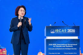
- After years away from the spotlight following US sanctions, Huawei’s legendary “chip queen”, He Tingbo – Huawei Board Director and President of its Semiconductor Business – has re-emerged to unveil the Tau (τ) Scaling Law, signaling a bold new chapter in China’s semiconductor ambitions. As the architect behind Hisilicon’s Kirin smartphones, Ascend AI accelerators, and Kunpeng server processors, her leadership underscores the growing importance of semiconductor R&D, talent, and technological resilience in the AI era.
- Huawei’s Tau (τ) Scaling Law proposes an alternative path to semiconductor scaling by focusing on time scaling – minimizing the latency of signals and data movement across chips and systems = rather than relying solely on geometric transistor shrinkage. Through multi-wafer stacking and system-level optimization, Huawei projects transistor density equivalent to 1.4nm processes by 2031, potentially extending semiconductor scaling beyond Moore’s Law.
- Semiconductor scaling economics are evolving as Moore’s Law faces rising fabrication costs and physical constraints. The τ scaling framework optimizes resistance and parasitic capacitance at the device level while leveraging vertically stacked LogicFolding architectures to shorten data pathways, reduce signal propagation delays, and improve energy efficiency.
- China’s push for semiconductor self-sufficiency continues to accelerate amid ongoing technology restrictions. Domestic investments across chip design, EDA software, materials engineering, manufacturing ecosystems, and advanced packaging are reshaping global supply chains.
- AI workloads require significantly greater computing power, memory bandwidth, and energy efficiency. Semiconductor companies capable of integrating AI accelerators with advanced packaging solutions may gain substantial competitive advantages in the era of generative AI.
- Semiconductor innovation is shifting beyond transistor density toward system-level optimization involving interconnects, photonics, software-hardware co-design, and packaging technologies. Huawei’s chip-level co-design approach integrates software, architecture, and silicon to improve workload parallelism and execution time, reinforcing the growing importance of heterogeneous integration.
- Global capital expenditure across semiconductor fabs, OSATs, substrate suppliers, and equipment manufacturers continues to rise as nations compete for AI leadership. Supply chain resilience and localization strategies are becoming strategic priorities as governments seek technological sovereignty.
- Advanced packaging is emerging as one of the most critical segments within the semiconductor value chain. System-level fabrics such as UnifiedBus with unified memory addressing and native memory semantics could drastically lower inter-chip and inter-rack communication latency, enabling next-generation AI computing and high-performance systems.
- Hyperscalers and cloud providers are increasing investments in custom silicon to support generative AI applications. Demand for AI accelerators, high-bandwidth memory, chiplets, and heterogeneous integration technologies is expected to remain robust over the coming decade.
- Asia-Pacific employment demand is expected to increase significantly as semiconductor manufacturing, AI infrastructure, and advanced packaging investments expand across China, Singapore, Taiwan, South Korea, and Southeast Asia. Rising demand for engineers, packaging specialists, manufacturing professionals, and senior leadership talent could intensify competition across the region.
Facing challenges hiring senior executives and skilled engineers fast enough to scale or dealing with semiconductor packaging constraints?
We connect you with best-fit senior leadership talent, professionals, and technical experts to strengthen your organisation.
We likewise deliver high-quality carrier tapes, cover tapes, reels, and thermoforming trays tailored for the industry’s most in-demand and advanced packages – from PDIP, SOIC, and QFNs to WLCSP, chiplets, modules, and panels.
- For enquiries or more information, DM us on WhatsApp: https://bit.ly/4nMk0G4 or visit our website at https://tmbsconsulting.com.
- TMBS Consulting – Your Semiconductor Concierge Talent Solutions | Packaging Solutions | Integrated Digital Solutions
#SemiconductorManufacturing #AIHardware #Chiplets #HPC #OSAT #SupplyChain #TalentAcquisition #ElectronicsManufacturing #AdvancedSemiconductorPackaging #ArtificialIntelligence