• Home
  • About Us
  • Breaking News
  • Semiconductor Insights
  • Contact Us
  • Talent Solutions
  • Packaging Solutions
  • Integrated Digital Services

Wafer Baking in Photoresist Photolithography

by admin | Oct 2, 2026 | Breaking News, Uncategorized

What It Really Takes to Build an AI Chip: Inside the World’s Most Complex Engineering Challenge

What It Really Takes to Build an AI Chip: Inside the World’s Most Complex Engineering Challenge

by admin | Aug 5, 2026 | Uncategorized

The 63rd Design Automation Conference (DAC 2026) gathered the global semiconductor industry from July 26–29, 2026, at the Long Beach Convention Center in Long Beach, California, USA, where the world’s leading experts in Electronic Design Automation (EDA),...

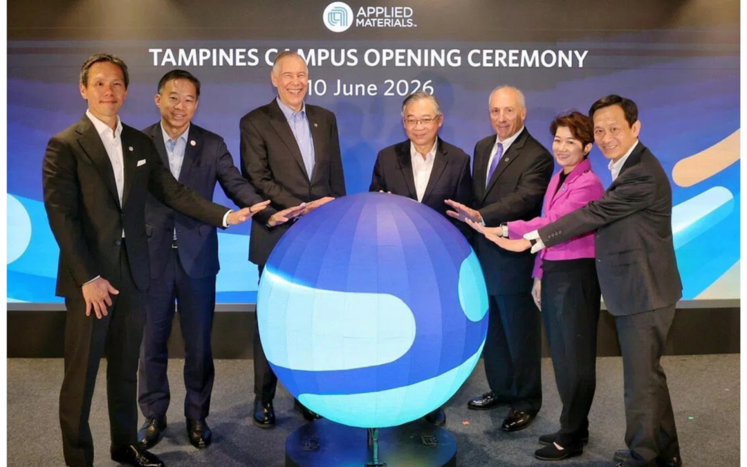
Semicon Giant Applied Materials Opens US$500m Singapore Plant, Adds 1,000 Jobs

Semicon Giant Applied Materials Opens US$500m Singapore Plant, Adds 1,000 Jobs

by admin | Jun 11, 2026 | Uncategorized

Kyle Christopher Borch, Micro-Mechanics CEO: The Architect of Precision in a World of Infinite Scale

Kyle Christopher Borch, Micro-Mechanics CEO: The Architect of Precision in a World of Infinite Scale

by admin | Feb 13, 2026 | Uncategorized

Kyle Christopher Borch, CEO of Micro-Mechanics (Holdings) Ltd., is the strategic architect behind a global precision engineering operation spanning Singapore, Malaysia, China, the Philippines, and the United States. Under his leadership, the company designs and...
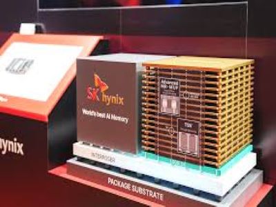
SK Hynix: Advancing High-Bandwidth Memory (HBM) for the Future of Compute

SK Hynix: Advancing High-Bandwidth Memory (HBM) for the Future of Compute

by admin | Feb 12, 2026 | Uncategorized

SK Hynix is transforming the memory industry with high-bandwidth HBM modules that stack multiple dies to meet the surging demands of AI accelerators, HPC systems, and next-generation data centers. SK Hynix is investing 19 trillion won (about $13 billion) to build a...
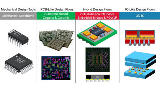
Inside the Advanced Packaging Matrix Powering the Future of AI, Chiplets, and Semiconductor Manufacturing

Inside the Advanced Packaging Matrix Powering the Future of AI, Chiplets, and Semiconductor Manufacturing

by admin | Feb 10, 2026 | Uncategorized

As transistor scaling slows, advanced semiconductor packaging has emerged as the decisive lever for performance, power efficiency, and system-level integration. The SemiconductorX Advanced Packaging Matrix Fan-out technologies such as InFO, FOWLP, and WLCSP are...

« Older Entries

Recent Posts

  • Filtronic Wins $68.1 Million SpaceX Deal: GaN Technology to Power Satellite Communications
  • Wafer Baking in Photoresist Photolithography
  • TSMC To Build 6 More Fabs in Texas?
  • TSMC Reaches the Atomic Frontier: The 0.42-Nanometer Interface That Could Redefine Transistor Scaling
  • SPIL’s $3.1 Billion Bet: Taiwan Builds Next Engine of AI Semiconductor Boom with CoWoS, Set to Create 2,000+ Jobs

Recent Comments

No comments to show.
  • Follow
  • Follow
  • Follow
  • Follow
  • Follow
  • Follow
  • Follow

Office Address

Canberra Crescent, Singapore 752119

Contact Us

  • richard.olivas@tmbsconsulting.com

© Copyright 2024 TMBS Consulting. All Rights Reserved.