
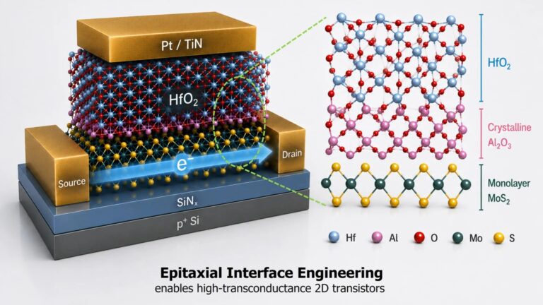
- Researchers at National Yang Ming Chiao Tung University and TSMC Corporate Research have engineered a 0.42-nanometer aluminum-oxide interface that protects electron transport in monolayer MoS₂ transistors while enabling strong gate control. The work addresses one of the most difficult problems in two-dimensional semiconductor devices: creating an ultrathin dielectric interface that improves electrostatic control without damaging the atomic-scale channel beneath it.
- The underlying challenge begins with transistor scaling itself. As conventional silicon devices become smaller, maintaining electrostatic control over the channel while limiting leakage, short-channel effects and power consumption becomes increasingly difficult, creating interest in semiconductor materials that can operate at atomic-scale dimensions.
- Monolayer molybdenum disulfide, or MoS₂, is attractive because its semiconductor channel can be only one atomic layer thick while retaining useful electronic properties. However, its surface is fundamentally different from conventional silicon, creating difficulties when engineers attempt to build the insulating gate-dielectric layer above it.
- A field-effect transistor uses a gate electrode to control the flow of current through a semiconductor channel, with an insulating dielectric separating the gate from that channel. Making the dielectric electrically thinner—measured through equivalent oxide thickness, or EOT—can strengthen electrostatic gate control, but an aggressively scaled dielectric can also introduce defects, charge traps, leakage and carrier scattering.
- MoS₂ presents a particularly difficult interface problem because its van der Waals surface does not provide the same chemical bonding environment found in conventional silicon surfaces. As a result, dielectric materials may struggle to nucleate into a uniform film, potentially producing electrical disorder that compromises the very carrier-transport advantages that make two-dimensional semiconductors attractive.
- The TSMC and university research team approached the interface as an engineered device layer rather than merely a boundary between two materials. An ultrathin epitaxial aluminum layer was deposited directly on CVD-grown monolayer MoS₂ and oxidized to create approximately 0.42 nanometers of aluminum oxide, followed by deposition of a high-κ hafnium oxide dielectric.
- The aluminum-oxide layer performs two important functions: it provides a smoother, more continuous surface for the hafnium oxide to grow on, while also acting as an atomic-scale buffer that reduces undesirable interactions between the high-κ dielectric and the MoS₂ channel. The resulting structure achieved an EOT of approximately 1 nanometer, combining strong gate control with preserved electron transport.
- The experimental devices were short-channel, top-gate MoS₂ transistors with channel lengths near 100 nanometers. They achieved maximum transconductance of approximately 0.45 millisiemens per micrometer, together with low gate leakage and minimal hysteresis; transconductance indicates how effectively changes in gate voltage modulate channel current.
- The significance of the 0.42-nanometer figure requires precision: it is not the gate length or a 0.42-nanometer transistor process node. It represents the thickness of the engineered aluminum-oxide interface, making the achievement important as an interface-engineering advance that could help remove a major obstacle to scaling atomically thin semiconductor channels.
- For the semiconductor industry, the development points toward a future in which scaling may depend increasingly on the engineering of materials, interfaces and process integration rather than dimensional shrinking alone. For professionals, that evolution expands the technology landscape around advanced materials, device engineering, process development, reliability, equipment, manufacturing and integration—areas where specialized technical expertise can become a significant competitive asset as emerging transistor architectures move from laboratory research toward manufacturable technologies.
Source: SemiWiki — “A 0.42 Nanometer Breakthrough from TSMC Could Push Transistors Beyond Silicon”
TMBS Consulting — Your Semiconductor Concierge
At TMBS Consulting, we connect organizations with the best-fit Senior Management leaders, Professionals, and Technical Staff to strengthen engineering capability, manufacturing excellence, and business growth—from advanced packaging and semiconductor manufacturing to emerging technologies such as panel-level packaging.
We also deliver high-quality carrier tapes, cover tapes, reels, and thermoforming trays tailored for the industry’s most in-demand and advanced semiconductor packages—from PDIP, SOIC, QFN, and WLCSP to chiplets, modules, and panel-level packaging.
🌐 https://tmbsconsulting.com 📩 DM us today.
#TSMC #Semiconductor #MoS2 #TwoDimensionalSemiconductors #TransistorTechnology #AdvancedSemiconductors #SemiconductorManufacturing #FutureOfSemiconductors #SemiconductorTechnology #ExecutiveSearch