
SK Hynix is transforming the memory industry with high-bandwidth HBM modules that stack multiple dies to meet the surging demands of AI accelerators, HPC systems, and next-generation data centers. SK Hynix is investing 19 trillion won (about $13 billion) to build a dedicated advanced packaging facility (P&T7) in Cheongju, boosting capacity for high‑bandwidth memory (HBM) and linking front‑end DRAM production to back‑end finishing, reflecting its commitment to meet surging AI‑memory demand.#AI #HighBandwidthMemory #HBM #SKHynix #MemoryInnovation
- SK Hynix has revolutionized memory production with HBM stacking technologies that deliver unprecedented bandwidth and reliability for AI and HPC workloads. Multi-die integration and thermal optimization have set new industry standards.
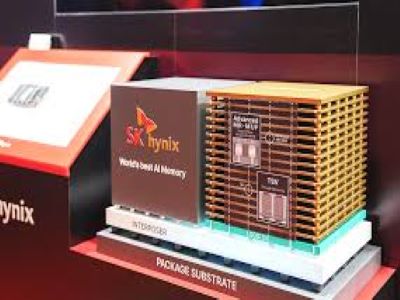
- The $13 billion Cheongju P&T7 facility integrates wafer fabs with advanced packaging and testing, creating a seamless ecosystem from fabrication to finished HBM modules. The scale demonstrates the premium placed on AI-focused memory solutions.
- As AI and HPC workloads grow, conventional DRAM and DDR5 outputs are constrained, highlighting HBM’s central role in next-generation compute. Lead times for standard memory products are extending, signaling structural shifts in the memory supply chain.
- Innovations in HBM3E and stacked memory allow SK Hynix to achieve higher bandwidth per module, enabling faster AI inference and training cycles with improved energy efficiency. Collaborative design with leading logic fabs further enhances system-level performance.
- Partnerships with TSMC and other logic fabs enable co-designed memory and compute modules, delivering unmatched performance for hyperscalers and cloud providers. This collaboration defines a new paradigm of memory integration in AI infrastructure.
- Competitors like Samsung and Micron are accelerating their roadmaps to keep up, intensifying the premium HBM market while driving innovation across the memory hierarchy. SK Hynix’s early lead ensures a durable advantage in high-performance memory.
- Global supply chains are shifting as secure AI memory supply becomes critical. Regional packaging and fab clusters strengthen technological leadership while mitigating geopolitical risks.
- SK Hynix has emerged as a full-stack AI memory provider, shaping product design, system integration, and architectural innovation. OEMs and hyperscalers rely increasingly on this integrated expertise to deliver differentiated AI platforms.
- Adoption of HBM4 and next-gen stacked memory expands SK Hynix’s influence in premium AI and HPC markets, while scaling production without compromising yield or reliability remains a key challenge. Market trends suggest sustained demand even as competition increases.
- In Asia-Pacific, SK Hynix’s expansion is creating significant opportunities for advanced packaging engineers, HBM process specialists, and senior technical leaders, fueling high-value employment in Korea, Taiwan, and Singapore. The growth of AI-centric memory is reshaping talent demand in the region.
Facing advanced semiconductor packaging constraints or difficulty hiring senior executives and skilled engineers fast enough to scale?
We deliver high-quality carrier tapes, cover tapes, reels, and thermoforming trays tailored for the industry’s most in-demand and advanced packages — from PDIP, SOIC, and QFNs to WLCSP, chiplets, modules, and panels.
At the same time, we connect you with the best-fit Senior Management leaders, Professionals, and Technical Staff to strengthen your organisation.
For enquiries or more information, please visit https://tmbsconsulting.com or contact Richard Chuck Olivas via WhatsApp: https://wa.me/6583393490
#AI #HighBandwidthMemory #HBM #SKHynix #SemiconductorIndustry #MemoryTechnology #AdvancedPackaging #TechLeadership #AsiaPacific #Chiplets