
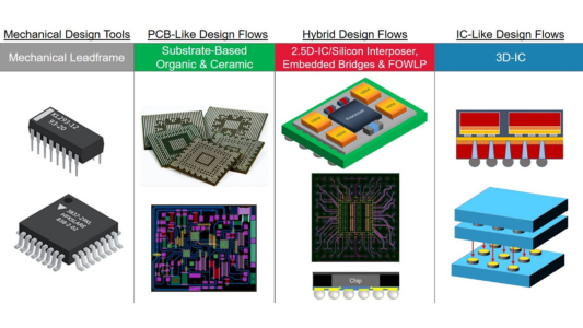
As transistor scaling slows, advanced semiconductor packaging has emerged as the decisive lever for performance, power efficiency, and system-level integration. The SemiconductorX Advanced Packaging Matrix
- Fan-out technologies such as InFO, FOWLP, and WLCSP are driving adoption in high-volume markets by delivering thinner profiles, lower parasitics, and cost-efficient scalability for mobile, RF, and consumer electronics.
- 2.5D and 3D architectures, including EMIB, CoWoS, and Foveros, are enabling high-bandwidth chiplet integration where performance, latency, and yield optimization directly impact AI and data-center economics.
- Advanced packaging has evolved into a strategic differentiator, with packaging capacity now influencing product roadmaps, time-to-market, and long-term customer commitments.
- Companies investing early in heterogeneous integration and advanced substrates are better positioned to capture premium ASPs as AI accelerators and HPC demand outpaces traditional SoC scaling.
- Across Asia-Pacific, advanced packaging expansion is accelerating demand for packaging engineers, process integration experts, equipment specialists, and senior technical leaders, reshaping employment trends in Taiwan, Korea, Singapore, and emerging Southeast Asian OSAT hubs.
Advanced Packaging Matrix
Source: SemiconductorX – Advanced Packaging Matrix
| Packaging Type | Category | Integration Style | Key Applications | Cost / Complexity |
| WLCSP | Wafer-Level | Die-level packaging | Mobile, sensors, PMICs | Low |
| FOWLP | Fan-Out | Wafer-level fan-out | RF, automotive, IoT | Low–Medium |
| InFO | Fan-Out | Advanced fan-out | High-end mobile SoCs | Medium |
| Flip-Chip BGA | Substrate-Based | Organic substrate | CPUs, GPUs | Medium |
| 2.1D (Organic Interposer) | Advanced | Partial interposer | Networking, ASICs | Medium |
| CoWoS | 2.5D | Full silicon interposer | AI accelerators, HPC | High |
| EMIB | 2.5D | Embedded silicon bridge | Chiplets, FPGAs | Medium |
| Foveros | 3D | Vertical die stacking | CPUs, AI processors | High |
| Panel-Level Packaging (PLP) | Fan-Out | Large-format integration | Future high-volume scaling | Medium–High |
Facing advanced semiconductor packaging constraints or difficulty hiring senior executives and skilled engineers fast enough to scale?
We deliver high-quality carrier tapes, cover tapes, reels, and thermoforming trays tailored for the industry’s most in-demand and advanced packages — from PDIP, SOIC, and QFNs to WLCSP, chiplets, modules, and panels.
At the same time, we connect you with the best-fit Senior Management leaders, Professionals, and Technical Staff to strengthen your organisation.
For enquiries or more information, please visit https://tmbsconsulting.com or contact Richard Chuck Olivas via WhatsApp: https://wa.me/6583393490
#AdvancedPackaging #SemiconductorIndustry #ChipletArchitecture #HeterogeneousIntegration #AIHardware #OSAT #Foundry #SemiconductorJobs #AsiaPacific #TechTalent