
Chinese researchers at Fudan University have developed a 1-nanometre Field-Programmable Gate Array (FPGA) using molybdenum disulfide (MoS₂) that can withstand radiation levels fatal to conventional silicon chips.
This breakthrough marks a major advance in 2D semiconductor technology and advanced packaging, with transformative potential for space, defense, and high-reliability industrial electronics worldwide.
hashtagSemiconductors hashtagAdvancedPackaging hashtag2DMaterials hashtagFPGA hashtagAerospaceTechnology hashtagRadiationHardened hashtagChiplets hashtagWLCSP hashtagDefenseTechnology hashtagInnovationLeadership
- Led by Professors Zhou Peng and Bao Wenzhong, Chinese researchers at Fudan University developed the world’s first radiation-resistant FPGA using 1-nanometre 2D molybdenum disulfide (MoS₂), capable of surviving extreme radiation that would destroy conventional silicon.
- This breakthrough advances 2D semiconductor technology and advanced packaging, with transformative potential for space, defense, and high-reliability industrial electronics.
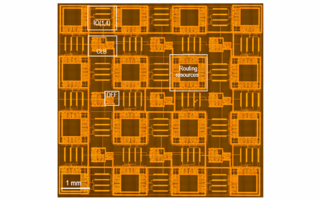
- An FPGA consists of configurable logic blocks, programmable interconnects, and memory arrays mounted on high-density substrates or ceramic packages. Its design enables high signal integrity and durability under reprogramming cycles, critical for mission-critical applications.
- The chip leverages 2D semiconductors, achieved by stacking atomically thin dies or layers to enhance power efficiency and reduce leakage. These layers – less than one nanometre thick – support high electron mobility and precise electrical control, essential for next-generation heterogeneous integration.
- Laboratory tests showed the circuits remained functional after exposure to 10 megarads of gamma radiation, levels that would destroy most silicon chips. This resilience makes it particularly valuable for satellites, deep-space probes, and military-grade systems operating in high-radiation environments.
- The development opens a new materials and packaging pathway that reduces reliance on heavy external shielding in space systems. By enhancing intrinsic chip robustness, it helps achieve lighter payloads, better energy efficiency, and higher system reliability.
- The atomic thinness of MoS₂ enables ultra-fast electron switching and dense vertical interconnects, advancing chiplet integration, fan-out wafer-level, and panel-level packaging. This supports compact, high-performance architectures for AI accelerators, radar systems, and communication modules.
- The research team previously achieved the world’s first all-2D semiconductor chip and the fastest flash memory, demonstrating compatibility with existing back-end processes and production lines. Their progress shows how material science and packaging innovation are converging to drive the post-silicon era.
- As 2D-based FPGAs transition from lab to production, they will transform advanced packaging and assembly supply chains, spurring innovation in thin-film stacking, high-density substrates, and heterogeneous interposers.
- Commercialization will expand demand for wafer bonding engineers, substrate designers, reliability analysts, and packaging specialists across China, Singapore, Taiwan, and South Korea.
Need efficient semiconductor packaging or top executive and technical talent? We deliver high-quality carrier tapes, cover tapes, reels, and thermoforming trays tailored for the industry’s most in-demand and advanced packages: from PDIP, SOIC, and QFNs to WLCSP, chiplets, modules, and panels. At the same time, we connect you with the best-fit Senior Management leaders, Professionals, and Technical Staff to strengthen your organisation. If this resonates, feel free to reach out: I personally check every message.
- Semiconductor Packaging Solutions (Carrier Tapes, Cover Tapes, Reels & Trays): https://bit.ly/3NdBhGB | chuck@superpak.com.sg
- For Leadership, Professional & Technical Talent, Remote Staffing: https://bit.ly/43myTXt | richard.olivas@tmbsconsulting.com
- For Digital & Software Solutions: richard.olivas@tmbsconsulting.com
- WhatsApp: +65 8339 3490
#Semiconductors #AdvancedPackaging #2DMaterials #FPGA #AerospaceTechnology #RadiationHardened #Chiplets #WLCSP #DefenseTechnology #InnovationLeadership