
ASE Technology Holding Co., Ltd. is spearheading the evolution of Fan-Out Panel-Level Packaging (FOPLP) and increasingly focusing on Fan-Out Chip-on-Substrate (FOCoS), positioning both as critical enablers of next-generation AI and HPC systems.
By scaling from wafer-level to panel-level packaging with FOPLP and progressively integrating multiple chiplets on substrates with FOCoS, ASE aims to achieve higher throughput, improved signal performance, and energy-efficient, high-density integration for advanced computing applications.
- ASE’s Fan-Out Panel-Level Packaging (FOPLP) expands from wafer to large panel formats, enabling higher productivity, lower cost, and greater design flexibility for AI/HPC devices. It’s a key solution for scaling production of high-performance and consumer electronics simultaneously.
- The company’s roadmap to scale production from 310 × 310 mm to 600 × 600 mm panels reinforces its leadership in moving from wafer-level to panel-level packaging. This transition supports higher-density integration while improving manufacturing efficiency.
- Panel-level manufacturing introduces challenges, such as controlling warpage, achieving precise redistribution layer (RDL) lithography, and ultra-fine die-to-panel alignment. ASE leverages advanced materials, automation, and process innovation to overcome these hurdles.
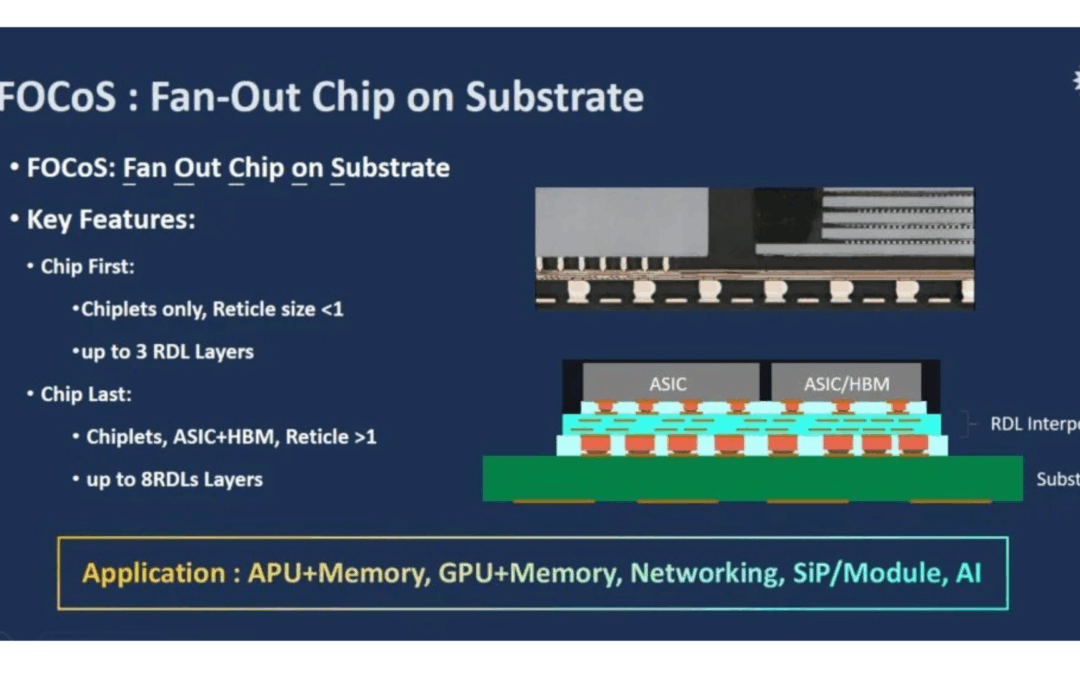
- While FOPLP addresses high-volume production, ASE is increasingly focusing on FOCoS for high-performance AI and HPC applications. FOCoS integrates multiple chiplets on a single substrate, shortening signal paths and enhancing speed, power efficiency, and thermal performance.
- FOCoS enables heterogeneous integration, combining logic, memory, and analog components within a single package. This allows AI servers, HPC clusters, and data centers to achieve high bandwidth, low latency, and energy efficiency.
- The dual-path strategy balances cost-efficient FOPLP production for consumer and IoT devices with FOCoS for performance-critical workloads. Together, they provide a roadmap from scalable manufacturing to next-gen system-level integration.
- Asia-Pacific continues to lead in FOPLP and FOCoS development, with Taiwan, Singapore, Malaysia, and South Korea at the center of R&D and industrial adoption. Local ecosystems support both manufacturing capabilities and talent growth.
- Reliable material handling and protective solutions are critical in advanced packaging processes. Proper management of components and panels helps maintain quality, prevent damage, and supports seamless FOPLP and FOCoS production.
- FOPLP and FOCoS are redefining competitiveness by enabling higher density, improved performance, and scalable manufacturing – changing how chips are designed, assembled, and delivered.
- These technologies are driving demand for engineers, R&D specialists, and senior technical leaders skilled in automation, materials science, and advanced packaging processes, creating high-value opportunities across the region.
Need efficient semiconductor packaging or top executive and technical talent? We deliver high-quality carrier tapes, cover tapes, reels, and thermoforming trays tailored for the industry’s most in-demand and advanced packages: from PDIP, SOIC, and QFNs to WLCSP, chiplets, modules, and panels. At the same time, we connect you with the best-fit Senior Management leaders, Professionals, and Technical Staff to strengthen your organisation. If this resonates, feel free to reach out: I personally check every message.
- For semiconductor packaging solutions (TnR & Thermoforming Trays): https://bit.ly/3NdBhGB | chuck@superpak.com.sg
- For leadership, professional, technical staff, & remote talent deployment: https://bit.ly/43myTXt | olivas@tmbsconsulting.com
- For digital ad software solutions: olivas@tmbsconsultiong.com
- WhatsApp Chuck Olivas: +65 8339 3490
#AdvancedPackaging #SemiconductorPackaging #FOPLP #FanOutPackaging #AIHPC #ChipletDesign #HeterogeneousIntegration #AsiaPacificTech #SemiconductorInnovation #PackagingTechnology