
Transistor technology is at a turning point as the world races to design faster, smaller, and more energy-efficient chips.
With global competition intensifying, atomic-level simulation is proving to be the hidden engine powering the shift from FinFET to Gate-All-Around devices.
hashtag#Semiconductor hashtag#TechInnovation hashtag#SupplyChain hashtag#Leadership hashtag#AsiaPacific
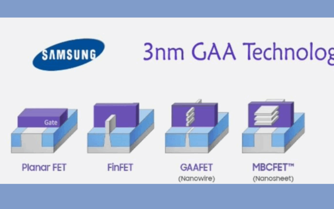
- FinFET, short for Fin Field-Effect Transistor, has been the workhorse of chip scaling for the past decade, enabling billions of transistors to fit into today’s smartphones and servers. Its vertical “fin” structure improves control of current flow, but it is now reaching physical and performance limits.
- Gate-All-Around devices replace the fin with channels fully surrounded by the gate, delivering superior electrostatic control and dramatically reducing energy leakage. This breakthrough architecture unlocks higher efficiency and performance in future chips.
- Atomic-level simulation allows researchers to model the movement of electrons inside these transistors with extreme precision. This approach helps avoid costly trial-and-error experiments during chip fabrication.
- Silvaco Inc’s advanced TCAD software replicates real material physics, including quantum effects, inside a virtual environment. Engineers can predict how new transistor structures will perform before manufacturing begins.
- By using virtual prototypes, chipmakers cut millions in R&D costs while reducing the risk of design flaws. This efficiency strengthens competitiveness in a market where speed-to-market defines winners.
- Process engineers gain the ability to test different materials and channel sizes virtually, finding the best balance between performance and manufacturability. That flexibility ensures new designs can scale into high-volume production.
- Accurate modeling of variability and stress factors improves transistor reliability for demanding applications such as AI, cloud data centers, and 5G infrastructure. Reliability is critical to maintaining customer trust and market share.
- EDA companies offering atomic-level simulation are expanding their role in the semiconductor ecosystem. They are evolving from tool providers to strategic partners driving innovation and profitability.
- Broader adoption of Gate-All-Around devices ensures faster innovation cycles, higher production yields, and stronger intellectual property protection across the semiconductor industry. These improvements accelerate global growth and competitiveness.
- Asia-Pacific employment demand rises as foundries and design companies require experts in simulation, materials science, and device engineering. This trend creates new opportunities for skilled professionals in Singapore, Taiwan, and Malaysia.
Need efficient semiconductor packaging or top executive and technical talent? We deliver high-quality carrier tapes, cover tapes, reels, and thermoforming trays tailored for the industry’s most in-demand and advanced packages – from PDIP, SOIC, and QFNs to WLCSP, Chiplets, modules, and panels. At the same time, we connect you with the best-fit Senior Management leaders, Professionals, and Technical Staff to strengthen your organization. And if you’re looking to boost visibility, engagement, and growth, we also provide Digital, Social, and Content Marketing solutions tailored to your business. If this resonates, feel free to reach out – I personally check every message.
- For packaging solutions: https://bit.ly/3NdBhGB | chuck@superpak.com.sg
- For leadership, technical talent and remote staffing needs: https://bit.ly/43myTXt | richard.olivas@tmbsconsulting.com
- For digital, social, and content marketing: richard@vector9.in
- WhatsApp Chuck Olivas at +65 8339 3490
#Semiconductors, #Electronics, #AI, #Technology, #Manufacturing, #SupplyChain, #Engineering, #Jobs, #Hiring, #Recruiting