
hashtag#chiplets hashtag#semiconductor hashtag#UCIe hashtag#heterogeneousintegration hashtag#3Dpackaging
- In a recent Semiconductor Engineering panel discussion held virtually, industry leaders Kurt Shuler (@Kurt Shuler LLC), Ravi Mahajan (Intel Corporation), Shekhar Kapoor (Amkor Technology, Inc.) , and Mike Kelly (ASE Global) gathered to explore the evolving chiplet landscape. They emphasized that while momentum is building, significant challenges remain around technical integration and die-to-die interoperability across vendors.
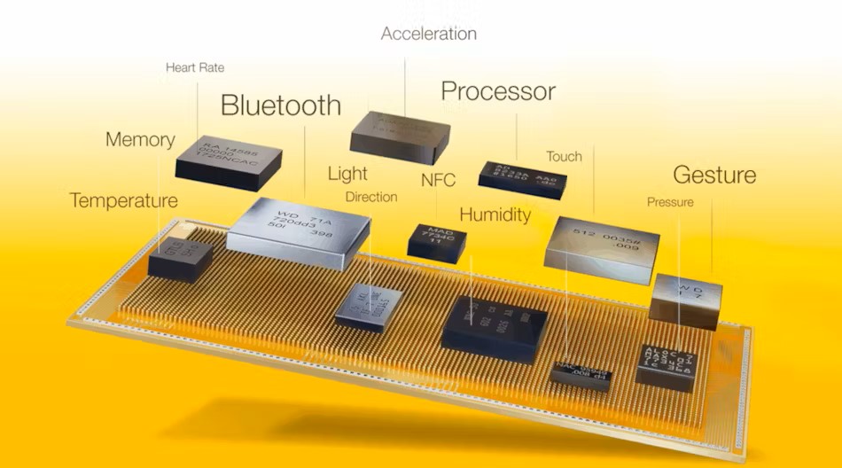
- Open standards such as UCIe (Universal Chiplet Interconnect Express), which enables seamless chiplet communication, BoW (Bunch of Wires), a flexible parallel-wire interface, AIB (Advanced Interface Bus), focusing on power-efficient, high-speed chiplet connections, and OpenHBI (Open High Bandwidth Interface), designed for dense data transfer, are gaining traction. These protocols reduce integration complexity and lower costs.
- Industry leaders are addressing physical integration challenges including probe/test methods and robust packaging design, essential for reliable heterogeneous and homogeneous chiplet systems. Packaging complexity currently limits scaling.
- Economic models now compare chiplet modularization versus monolithic designs, highlighting trade‑offs in yield, cost per die, and time‑to‑market. Executives are using these frameworks to drive decision‑making in product roadmaps.
- Foundries and IP suppliers are exploring chiplet offerings that enable reuse of specialized IP blocks. This modular strategy boosts design flexibility and lowers non‑recurring engineering costs in specialized chips.
- Pilot implementations, especially in AI accelerators and high‑performance computing, demonstrate technical feasibility and attract investment for chiplet adoption at scale. Investors are increasingly funding startups focused on chiplet-based architectures.
- Consortia and industry alliances are pushing toward a neutral marketplace, but full standard compliance and certification regimes are still under development. Without these, cross‑vendor integration remains difficult.
- Adoption by hyperscalers and cloud providers is helping validate commercial viability, though broader ecosystem maturity is needed to support volume production and supply chain robustness.
- The emergence of a robust chiplet ecosystem will catalyze the semiconductor industry’s growth. By enabling modular, scalable designs and reducing cost barriers, chiplet-based architectures are positioned to expand market scope and increase industry innovation capacity.
- The shift toward chiplets will boost Asia‑Pacific employment. As design, integration, packaging and testing ecosystems develop in countries like Taiwan, Korea, Japan, India and Singapore, demand for skilled engineers and manufacturing talent will rise sharply.
Do you need a more efficient semiconductor packaging solution or are you struggling to find best-fit candidates for executive, professional, or technical roles? We’re here to help as your trusted consultant.
From carrier tapes and cover tapes to thermoforming trays for large package sizes, modules and panels, our technologies are designed to handle the full spectrum of semiconductor package types – covering legacy formats like WLCSP, BGA, QFP, SSOP, TSOP, and PDIP, as well as advanced architectures such as Fan-Out, 2.5D/3D IC, and Chiplet Integration.
- For packaging solutions: https://bit.ly/3NdBhGB
- For leadership and technical talent needs: https://bit.ly/43myTXt
- Contact: chuck@superpak.com.sg | richard.olivas@tmbsconsulting.com
#semiconductormanufacturing #SemiconductorSolutions #executivesearch #technicalrecruitment #hiringprofessionals #semiconductorgrowth
Experts highlight technical progress, commercialization pathways, and the broader impact on growth and employment across Asia‑Pacific.