
Introduction
As transistor scaling slows and Moore’s Law delivers diminishing returns, semiconductor advanced packaging has emerged as the primary driver of performance, power efficiency, and system-level differentiation. From AI accelerators to chiplet-based architectures, packaging technologies now determine bandwidth, latency, yield, and cost structures across the semiconductor value chain.
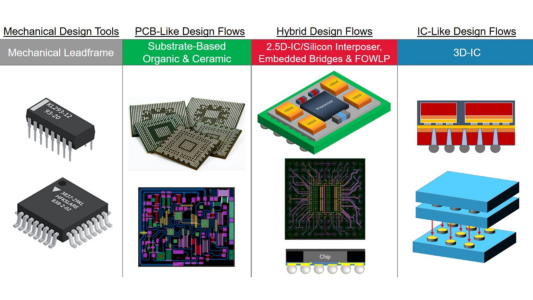
The Advanced Packaging Matrix highlights how fan-out, 2.5D, and 3D integration approaches—such as InFO, FOWLP, CoWoS, EMIB, and Foveros—are redefining chip design economics and global competitiveness.
What Is Semiconductor Advanced Packaging?
Semiconductor advanced packaging refers to next-generation integration technologies that go beyond traditional wire-bond and flip-chip approaches. These methods enable higher I/O density, heterogeneous integration, and improved thermal and electrical performance by tightly coupling multiple dies, chiplets, and substrates into a single system-level solution.
(Featured snippet–optimized definition: ~45 words)
Why Semiconductor Advanced Packaging Matters for AI and HPC
AI and high-performance computing (HPC) workloads demand massive bandwidth, low latency, and power-efficient interconnects—requirements that conventional monolithic SoCs can no longer meet.
Advanced packaging enables:
-
Chiplet architectures that improve yield and design flexibility
-
High-bandwidth interconnects for AI accelerators and GPUs
-
System-level scaling without shrinking transistors
Technologies such as CoWoS, EMIB, and Foveros are now critical to AI data center economics, where packaging capacity directly impacts deployment timelines and total cost of ownership.
Key Takeaways from the Advanced Packaging Matrix
1. Fan-Out Packaging Drives High-Volume Adoption
Fan-out technologies including InFO, FOWLP, and WLCSP deliver thinner profiles, lower parasitics, and scalable cost structures. These solutions dominate mobile, RF, and consumer electronics markets while expanding into automotive and IoT.
2. 2.5D and 3D Architectures Enable Chiplet Economics
Advanced approaches such as CoWoS, EMIB, and Foveros allow designers to integrate logic, memory, and accelerators with optimized performance-per-watt. These architectures are foundational for AI accelerators, networking ASICs, and HPC platforms.
3. Packaging Has Become a Strategic Bottleneck
Advanced packaging capacity now influences:
-
Product roadmaps
-
Time-to-market
-
Long-term customer commitments
Foundries and OSATs investing early in substrates, interposers, and advanced assembly lines are gaining structural advantages.
4. Heterogeneous Integration Unlocks Premium ASPs
As AI and HPC demand outpaces traditional scaling, companies leading in heterogeneous integration are better positioned to capture premium average selling prices (ASPs) and long-term hyperscaler partnerships.
5. Talent Demand Is Accelerating Across Asia-Pacific
Expansion of advanced packaging is reshaping employment trends across Taiwan, Korea, Singapore, and Southeast Asia, driving demand for:
-
Packaging engineers
-
Process integration specialists
-
Equipment and yield experts
-
Senior technical and operations leaders
Semiconductor Advanced Packaging Matrix (Overview)
| Packaging Type | Category | Integration Style | Key Applications | Cost / Complexity |
|---|---|---|---|---|
| WLCSP | Wafer-Level | Die-level | Mobile, sensors, PMICs | Low |
| FOWLP | Fan-Out | Wafer-level fan-out | RF, automotive, IoT | Low–Medium |
| InFO | Fan-Out | Advanced fan-out | High-end mobile SoCs | Medium |
| Flip-Chip BGA | Substrate | Organic substrate | CPUs, GPUs | Medium |
| CoWoS | 2.5D | Silicon interposer | AI accelerators, HPC | High |
| EMIB | 2.5D | Embedded bridge | Chiplets, FPGAs | Medium |
| Foveros | 3D | Vertical stacking | CPUs, AI processors | High |
| PLP | Fan-Out | Panel-level | Future scaling | Medium–High |
Market Trends and Industry Context
Leading semiconductor players such as TSMC, Intel, Samsung, and advanced OSATs are expanding advanced packaging capacity to meet AI-driven demand. Panel-level packaging, next-generation substrates, and co-design between logic and packaging teams are emerging as critical differentiators.
The industry is transitioning from “design for silicon” to “design for system integration.”
FAQs – People Also Ask
What is semiconductor advanced packaging used for?
It enables high-performance, power-efficient integration of chiplets and heterogeneous dies for AI, HPC, automotive, and mobile applications.
Why is advanced packaging critical for AI chips?
AI workloads require high-bandwidth memory, low latency, and scalable interconnects that only advanced packaging can deliver.
Which regions lead in advanced semiconductor packaging?
Taiwan, Korea, and increasingly Singapore and Southeast Asia lead due to strong foundry, OSAT, and talent ecosystems.
Facing advanced semiconductor packaging constraints or difficulty hiring senior executives and skilled engineers fast enough to scale?
We deliver high-quality carrier tapes, cover tapes, reels, and thermoforming trays tailored for the industry’s most in-demand packages — from PDIP, SOIC, and QFNs to WLCSP, chiplets, modules, and panels.
At the same time, we connect you with best-fit Senior Management leaders, Professionals, and Technical Staff to strengthen your organization across manufacturing, packaging, and integration.
👉 https://tmbsconsulting.com
📱 WhatsApp Chuck Olivas: https://wa.me/6583393490