
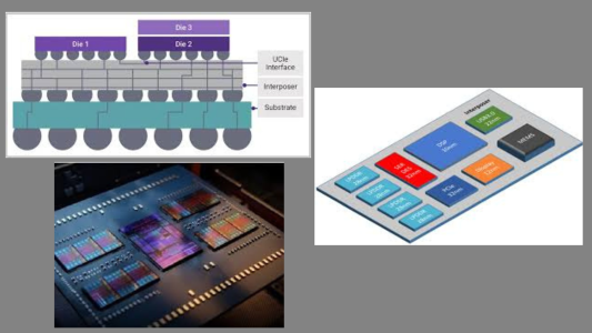
Chiplets are driving the next leap in compute capacity and I/O bandwidth by splitting SoC functionality into smaller heterogeneous or homogeneous dies integrated within a single system-in-package (SiP).
Leveraging substrates and interposers for higher routing density, SiPs enable unprecedented functionality and integration – making chiplet design choices a decisive factor in the industry’s future.
hashtagSemiconductor hashtagTechInnovation hashtagSupplyChain hashtagLeadership hashtagAsiaPacific
- The first design question is partitioning: teams must decide which functional blocks – compute, I/O, and memory – belong on separate chiplets, and then weigh trade-offs in latency, bandwidth, and power. This partitioning decision dictates how each block leverages the semiconductor process node best suited for performance and cost.
- Selecting the optimal process node for each chiplet enables heterogeneous integration, where compute may use advanced nodes while I/O and memory can leverage mature, lower-cost technologies. This strategy maximizes efficiency without overextending expensive advanced lithography.
- Packaging choice follows, with organic substrates delivering lower cost and faster schedules, while silicon or RDL interposers enable much higher interconnect density. Designers must balance schedule risk, electrical requirements, and system complexity.
- Within interposer solutions, mature silicon, RDL interposers, or RDL with silicon bridges each offer unique density, flexibility, and cost profiles. The right choice aligns with bandwidth requirements, die size constraints, and integration goals.
- Multi-die systems heighten mechanical and signal-integrity challenges, requiring detailed thermal analysis and power delivery modeling. Each chiplet must be verified not only in isolation but also for its interactions across the package.
- Bump-pitch planning is a critical step, with substrate bumps typically 110–150 µm and interposer microbumps as fine as 25–55 µm. As 3D stacking is added, complexity increases, demanding tighter alignment across chiplets.
- Yield success depends on rigorous test planning—designers must coordinate bump placement, probe access, and KGD (known-good die) flows. Standards such as IEEE 1838 enable robust multi-die testing even when pins are inaccessible.
- Security is a new frontier for chiplets: multi-die systems increase the attack surface, requiring authentication, attestation, and secure key transfers at boot time. Building a root of trust into each chiplet ensures integrity across heterogeneous designs.
- The rise of chiplet-based packaging is accelerating semiconductor growth by enabling scalable, modular system construction. Faster time-to-market, better yields, and higher integration density are reinforcing the industry’s long-term momentum.
- Across Asia-Pacific, chiplet design complexity is reshaping employment trends, fueling demand for packaging engineers, interconnect specialists, and semiconductor security architects. Companies are competing aggressively for talent to support this next wave of innovation.
Need efficient semiconductor packaging or top executive and technical talent? We deliver high-quality carrier tapes, cover tapes, reels, and thermoforming trays tailored for the industry’s most in-demand and advanced packages – from PDIP, SOIC, and QFNs to WLCSP, Chiplets, modules, and panels. At the same time, we connect you with the best-fit Senior Management leaders, Professionals, and Technical Staff to strengthen your organization. If this resonates, feel free to reach out – I personally check every message
- For packaging solutions: https://bit.ly/3NdBhGB
- For leadership and technical talent needs: https://bit.ly/43myTXt
- Contact: chuck@superpak.com.sg | richard.olivas@tmbsconsulting.com
- WhatsApp Chuck Olivas at +65 8339 3490
#Semiconductors, #Electronics, #AI, #Technology, #Manufacturing, #SupplyChain, #Engineering, #Jobs, #Hiring, #Recruiting