
Nexperia and TU Hamburg have launched an endowed professorship in power-electronic devices to accelerate SiC, GaN, and AlScN semiconductor development and strengthen talent pipelines for energy-efficient innovations. This strategic partnership will drive next-gen device architectures and advanced fault-prediction systems as part of a broader push toward electrification.
#semiconductors #powerelectronics #SiC #GaN #research
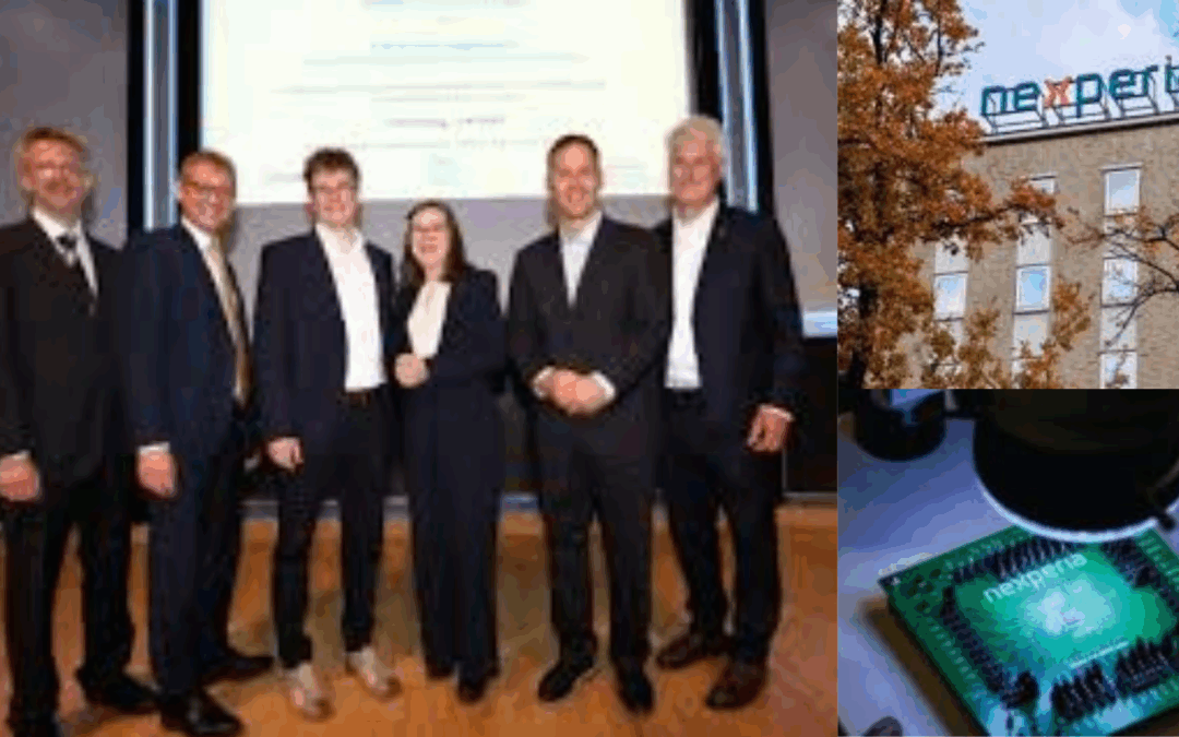
- Nexperia and TU Hamburg have established a new endowed chair, held by Prof. Holger Kapels, to lead the Institute for Power Electronic Devices focused on wide-bandgap innovation.
- The initiative targets Wide-Bandgap (WBG) compound semiconductors such as SiC, GaN, and AlScN that enable higher switching speeds, reduced conduction losses, and more compact modules ideal for EVs, data centers, and industrial systems.
- These WBG semiconductors offer superior electrical properties compared to traditional silicon, including higher voltage tolerance, faster switching speeds, and lower energy losses. These advantages make WBG devices critical for next-generation power electronics used in electric vehicles, data centers, and industrial applications, driving efficiency and performance gains across the semiconductor industry.
- Research will explore advanced architectures like vertical GaN FETs and leverage machine-learning techniques for predictive fault detection in power devices.
- The endowed chair reflects Nexperia’s long-term strategy to build local innovation capacity, capitalizing on its century-old Hamburg wafer-fab legacy.
- Nexperia’s Hamburg facility currently accounts for about 25% of the world’s small-signal diode and transistor production, with headcount rising from 950 to approximately 1,600 post-modernization.
- Company leadership emphasized that combining research and talent development is essential for strengthening Germany’s deep-tech semiconductor ecosystem.
- Prof. Kapels will teach core courses like ‘Electrical Engineering I’ and ‘Wide Bandgap Semiconductors’ from the winter semester 2025/26 to train the next generation of engineers.
- This partnership is expected to accelerate semiconductor innovation, enhancing industry growth through cutting-edge device R&D and workforce development.
- Asia-Pacific employment benefits indirectly as expanded global demand for power-electronics bolsters manufacturing-linked job creation and R&D roles across regional facilities.
Unlock cost-effective, high-quality semiconductor packaging solutions (including carrier tapes, cover tapes, and thermoforming trays) – for various package types. We support advanced architectures like Fan-Out, 2.5D/3D IC, and Chiplet Integration, as well as legacy formats such as WLCSP, BGA, QFP, SSOP, TSOP, and PDIP. Our thermoforming trays are ideal for large packages, modules, and panels. We’re here to support you every step of the way.
- Fill out this brief questionnaire: https://bit.ly/3NdBhGB
- Contact Chuck Olivas at chuck@superpak.com.sg for more info.
Struggling to secure top-tier Senior Management, Professionals or Technical staffing while key roles stay vacant, KPIs are missed / unmet, productivity stalls, and your team is overwhelmed by misaligned candidates and drawn-out hiring cycles?
TMBS Consulting specializes in the search and placement of Senior Management Team members, seasoned Professionals, and Technical experts, with a proven track record of delivering top-tier talent in manufacturing, engineering, logistics, IT, and finance.
- Share your hiring challenges here: https://bit.ly/43myTXt
- Contact Chuck Olivas at richard.olivas@tmbsconsulting.com – Let’s build your Dream Team.
#semiconductormanufacturing #SemiconductorSolutions #semiconductorjobs #semiconductorgrowth#ExecutiveSearch #LeadershipHiring #StrategicRecruitment #HiringTopTalent #CLevelRecruiting #semiconductors #semiconductorindustry