
Market Research Intellect forecasts that the global advanced chip packaging market will surge from approximately USD 50 billion in 2025 to nearly USD 80 billion by 2032, driven by demand for miniaturization, AI, 5G, EVs, and data-center expansion. Innovations in fan-out wafer-level, 3D/2.5D packaging, and heterogeneous integration are opening new revenue streams and capacity investments across key semiconductor regions.
#AdvancedPackaging #Semiconductors #AIChips #FanOut #3DIntegration
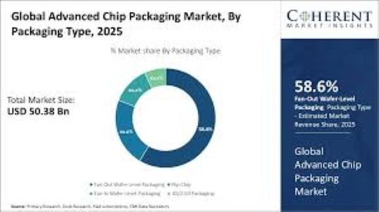
- The market is expected to grow at a 6.8% CAGR, with revenues increasing from USD 50.38 billion in 2025 to USD 79.85 billion by 2032. This growth is propelled by increasing demand for higher performance chips in compact form factors.
- Asia-Pacific leads with over 50% market share, supported by strong electronics and semiconductor manufacturing bases in China, Taiwan, South Korea, and Japan. Regional dominance is reinforced by government support, advanced supply chains, and skilled labor.
- North America is the fastest-growing region, driven by investments in data centers, electric vehicles, and AI-related chip packaging. U.S.-based foundries and fabless players are expanding advanced packaging capabilities domestically.
- Fan-out wafer-level packaging holds the largest share, while 3D ICs and 2.5D packaging are seeing the fastest growth due to their ability to enable higher performance and integration. These technologies support increased I/O density and power efficiency.
- Consumer electronics remain the top application, while automotive electronics—especially for EVs—are growing rapidly due to demand for reliable, thermally efficient packaging. This shift aligns with the global move toward electrification and smart mobility.
- The Internet of Things contributes a sizable portion of demand, and aerospace applications are also expanding as advanced packaging proves its viability in extreme conditions. Ruggedized and miniaturized solutions are key for satellite and avionics systems.
- Average selling prices for wafer-level packaging are rising, driven by increasing costs of substrates and materials, as well as growing demand for higher-density chips. This is contributing to stronger margins for packaging service providers.
- Patents related to heterogeneous integration are increasing, signaling a technological shift toward integrating logic and memory dies for AI, telecom, and high-performance computing. This innovation allows for faster data processing and better system efficiency.
- Advanced chip packaging is playing a pivotal role in the semiconductor industry’s long-term growth by enabling smaller, faster, and more energy-efficient devices. It is also helping mitigate supply chain vulnerabilities through localized, value-added processes.
- Asia-Pacific employment is expected to rise significantly as packaging investments expand in the region. New jobs in R&D, engineering, quality assurance, and factory automation will support this momentum
Frustrated by rising packaging costs, inconsistent quality, or unresponsive customer support? Unlock cost-effective, high-quality semiconductor packaging solutions for your various package types from advanced architectures like Fan-Out, 2.5D/3D IC, and Chiplet Integration to legacy types like WLCSP, BGA, QFP, SSOP, TSOP, and PDIP. We’re here to support you every step of the way.
- Fill out this brief questionnaire: https://bit.ly/3NdBhGB
- Contact Chuck Olivas at chuck@superpak.com.sg for more info.
Struggling to secure top-tier C-Suite or Professional / Technical talent while key roles stay vacant, KPIs are missed / unmet, productivity stalls, and your team is overwhelmed by misaligned candidates and drawn-out hiring cycles?
TMBS Consulting specializes in the search and placement of Senior Management Team members, seasoned Professionals, and Technical experts, with a proven track record of delivering top-tier talent in manufacturing, engineering, logistics, IT, and finance.
- Share your hiring challenges here: https://bit.ly/43myTXt
- Contact Chuck Olivas at richard.olivas@tmbsconsulting.com – Let’s build your Dream Team.
#ExecutiveSearch #LeadershipHiring #StrategicRecruitment #HiringTopTalent #CLevelRecruiting #semiconductors #semiconductorindustry #semiconductormanufacturing #SemiconductorSolutions #semiconductorjobs #semiconductorgrowth