
-
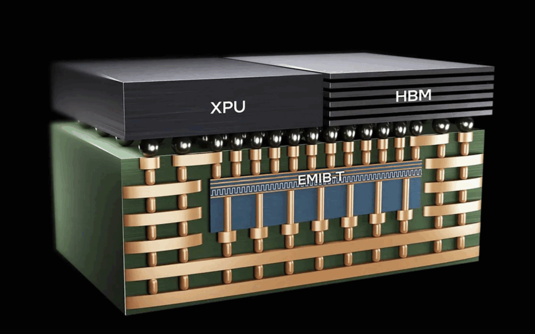
Intel Corporation, which first introduced its Embedded Multi-die Interconnect Bridge (EMIB) technology in 2017, has since evolved it into EMIB-T – an enhanced version designed for improved testability and scalability in multi-die packaging, particularly for high-performance computing (HPC), AI accelerators, and advanced SoCs.
-
EMIB‑T elevates die‑to‑die connectivity with high‑density horizontal interconnects and vertical through‑silicon vias, enabling over 38 bridges and packaging more than 10,000 mm² of silicon into a single unit.
-
A newly added copper ground‑plane grid enhances signal integrity and power delivery, reducing electrical noise and improving performance consistency for large-scale AI processing.
-
Compression bonding with low thermal gradient allows for die pitches as tight as 25 µm, increasing interconnect density and improving thermal alignment across massive chip assemblies.
-
Modular integrated heat spreaders are engineered with stiffeners to retain flatness under high thermal loads, ensuring uniform heat dissipation and mechanical stability across extended silicon.
-
The advanced packaging techniques now support package areas exceeding 21,000 mm²- more than four and a half credit cards—opening doors to massive AI processors with greater compute power.
-
This packaging evolution bypasses traditional reticle limits of ~800 mm², creating a path to larger chips with higher transistor counts without the need for monolithic die fabrication.
-
Future packages can integrate over a dozen full-size chiplets into one cohesive system, sharply boosting performance-per-watt and enabling ultra-fast AI data processing.
-
Improved thermal pathways from silicon to the heat spreader address reliability concerns, allowing chips to run longer at higher power densities without degradation.
-
Continued innovation in chiplet-based packaging positions Intel Foundry to compete head-to-head with TSMC in delivering AI-ready solutions, reinforcing leadership in semiconductor scalability.
-
Accelerated development in advanced packaging is poised to drive a new phase of growth in the semiconductor industry, supporting next-gen AI, HPC, and edge computing ecosystems.
-
Rising demand for packaging engineers, fab specialists, and materials scientists will expand employment opportunities across semiconductor hubs in Taiwan, Singapore, Malaysia, and South Korea.
Frustrated by rising packaging costs, inconsistent quality, or unresponsive customer support? Unlock cost-effective, high-quality semiconductor packaging solutions for your various package types from advanced architectures like Fan-Out, 2.5D/3D IC, and Chiplet Integration to legacy types like WLCSP, BGA, QFP, SSOP, TSOP, and PDIP. We’re here to support you every step of the way.
-
Fill out this brief questionnaire: https://bit.ly/3NdBhGB
-
Contact Chuck Olivas at chuck@superpak.com.sg for more info.
-
#SemiconductorPackaging #AdvancedPackaging #ChipManufacturing #WLCSP #ElectronicsManufacturing
Struggling to secure top-tier C-Suite or Professional talent while key roles stay vacant, KPIs are missed / unmet, productivity stalls, and your team is overwhelmed by misaligned candidates and drawn-out hiring cycles?
TMBS Consulting specializes in the search and placement of Senior Management Team members, seasoned Professionals, and Technical experts, with a proven track record of delivering top-tier talent in manufacturing, engineering, logistics, IT, and finance.
-
Share your hiring challenges here: https://bit.ly/43myTXt
-
Contact Chuck Olivas at richard.olivas@tmbsconsulting.com – Let’s build your Dream Team.
-
#ExecutiveSearch #LeadershipHiring #StrategicRecruitment #HiringTopTalent #CLevelRecruiting